Semiconductors · Vol. V|Photolithography|1960s (planar process)
Photolithography
1960s (planar process)
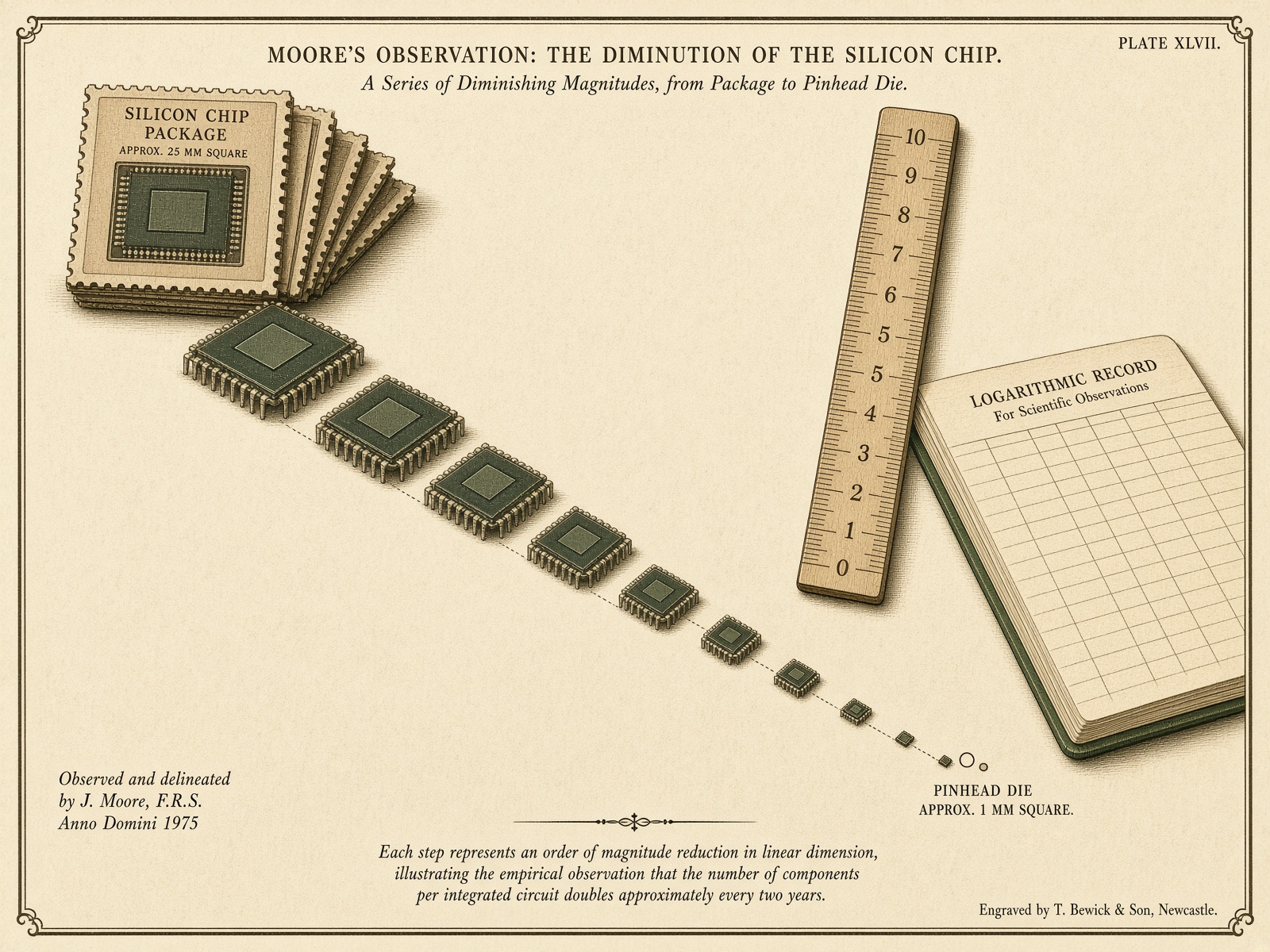
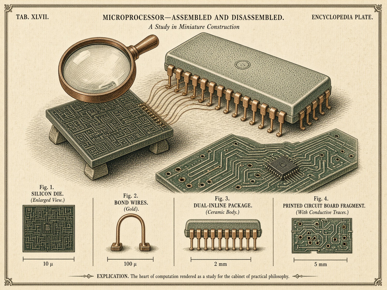
Chips are printed. Light (later ultraviolet, then EUV) shines through a mask onto photoresist; chemistry etches or deposits only where the pattern allows. Photolithography is why a billion transistors can share a fingernail. Each generation is a fight with wavelength, dust, and economics. The fab is a printing press for matter.
Fairchild and others (planar process lineage from Hoerni) · United States, then global fabs
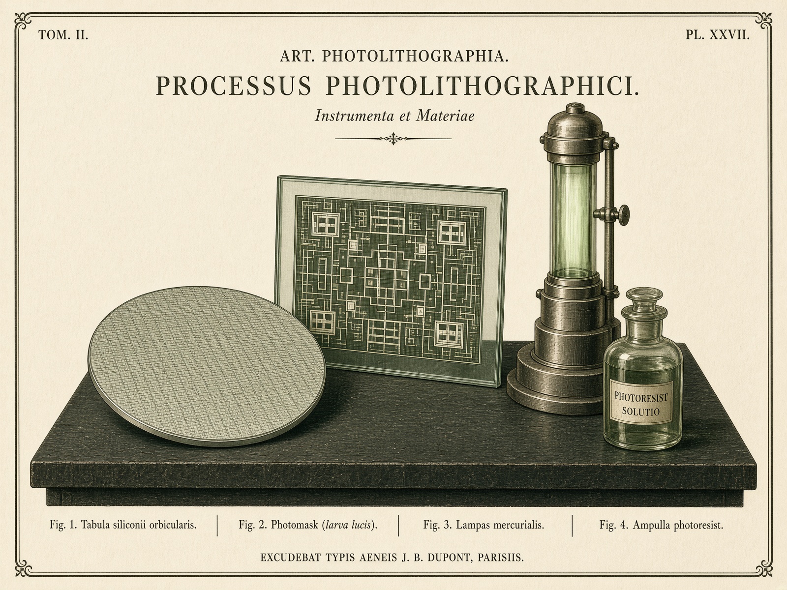
How the mechanism is arranged
How it works
- Coat the wafer with light-sensitive resist.
- Project a mask pattern; develop the resist.
- Etch, dope, or deposit in the openings; strip resist; repeat dozens of layers.
Why it mattered
- Turned circuit design into a reproducible print run.
- Set the pace of scaling.
- Concentrated manufacturing in a few extreme factories.
Who turned the wheel
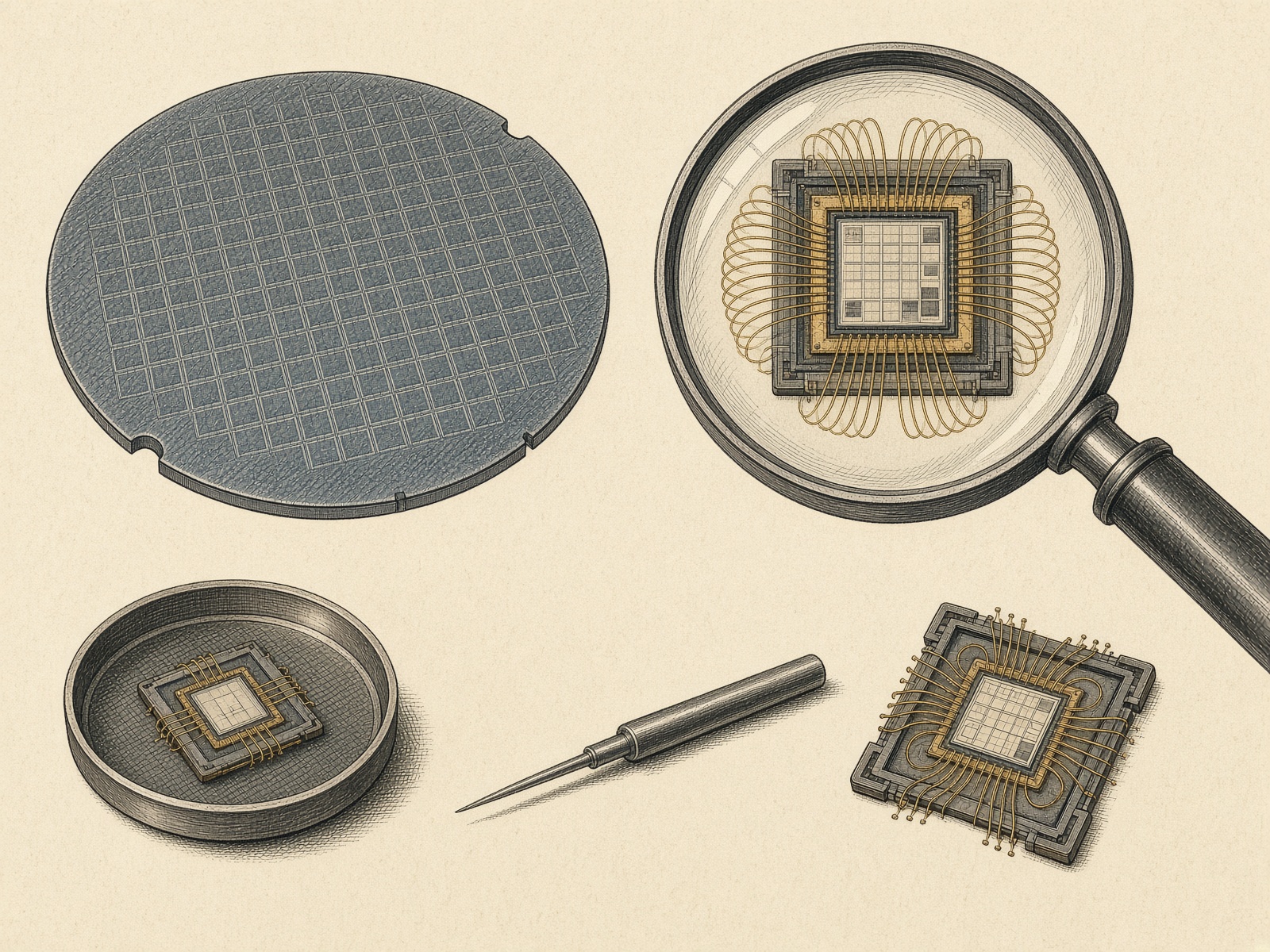
What it unlocked
For further study
- Hoerni planar patent lineage. Fairchild.
- ASML technical primers. Later lithography.
Check
What does the photoresist do in one sentence?